
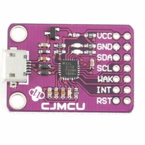
PCF8591 Converter Module
This is PCF8591 Converter Module a breakout board/Prototype Board for PCF8591 IC. The PCF8591 is a single-chip, single‑supply low‑power 8‑bit CMOS data acquisition device with four analog inputs, one analog output, and a serial I²C‑bus interface. Three address pins A0, A1, and A2 are used for programming the hardware address, allowing the use of up to eight devices connected to the I²C‑bus without additional hardware. Address, control, and data to and from the device are transferred serially via the two-line bidirectional I²C‑bus.
The functions of the device include analog input multiplexing, on-chip track and hold function, 8-bit analog‑to‑digital conversion, and an 8‑bit digital‑to‑analog conversion. The maximum conversion rate is given by the maximum speed of the I²C-bus.
PCF8591 IC Features:
- Single power supply
- A PCF8591 operating voltage range of 2.5V-6V
- Low standby current
- Via I2C bus serial input/output
- PCF8591 by 3 hardware address pins addressing
- PCF8591 I2C bus speed sampling rate decided
- 4 analog inputs programmable single-ended or differential input
- Automatic incremental channel selection
- PCF8591 analog voltage range from VSS to VDD
- PCF8591 built-in track-and-hold circuit
- 8-bit successive approximation A / D converter
- 1 analog output DAC gain
PCF8591 Converter Module Features:
- The PCF8591 Converter Module supports external voltage input of the 4-way acquisition (voltage input range of 0-5v)
- The PCF8591 Converter Module integrated photoresistor by AD collection precise value of the ambient light intensity
- Module integrated thermistor by the precise value of the ambient temperature of the AD acquisition
- Module integrated 1 channel 0-5V voltage input acquisition (the blue potentiometer to adjust the input voltage)
- Modules with power indicator (for the module power supply indicator lights)
- Modules with DA output indicator, when the module DA output interface voltage reaches a certain value, will be lit panel the DA output indicator, the higher the voltage, the more obvious indicator brightness
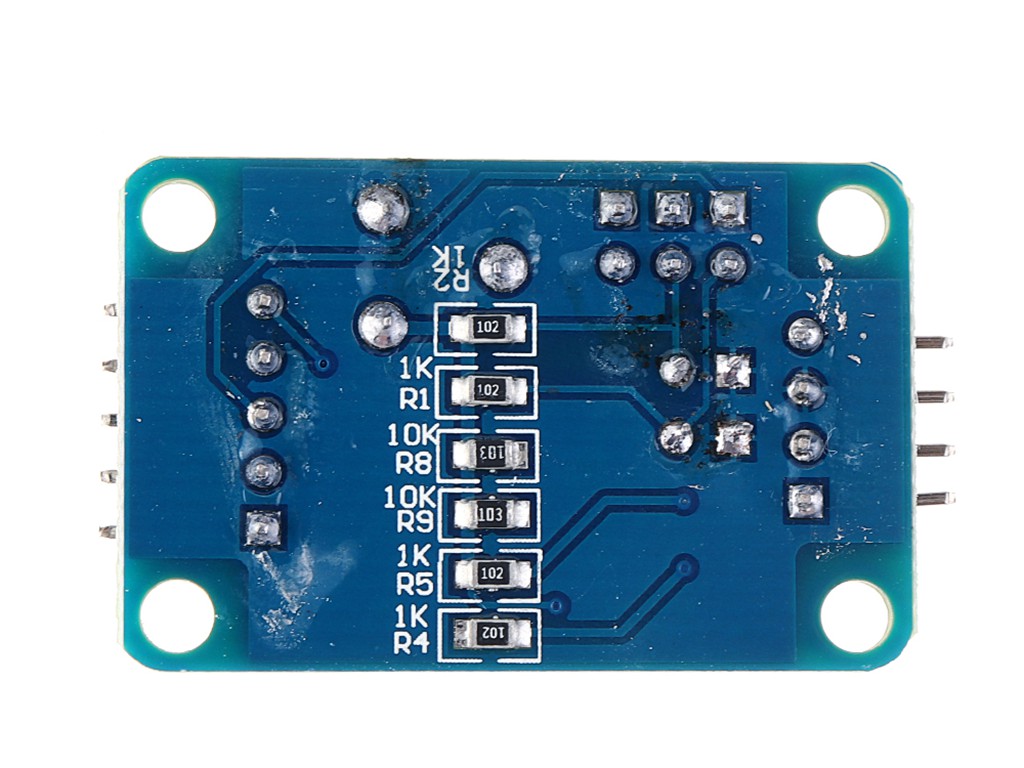
- Module PCB size: 3.6cm x 2.3cm
- A standard double panel, thickness 1.6mm, nice layout, surrounded by a through-hole, aperture: 3mm, convenient fixed.
Module interface specification:
The Left:
- AOUT chip DA output interface
- AINO chip analog input interface 0
- AIN1 chip analog input interface 1
- AIN2 chip analog input interface 2
- AIN3 chip analog input interface 3
The Right:
- SCL – IIC clock interface connected to microcontroller IO port
- SDA – IIC digital interface connected to microcontroller IO port
- GND – connected to ground
- VCC – connected to 3.3v-5v
- Four red jumper-cap instruction
- P4 – connected to P4 shorting cap, select thermistor access circuit
- P5 – connect P5 shorting cap, select photoresistor access circuit
- P6 – connected to P6 shorting cap, select 0-5V adjustable voltage access circuit

There are no reviews yet.